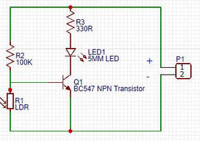
Now, once the PCBs have arrived, I can place it to use. After I have gained these following components for this PCB design, I can solder this kit up. You can also make this custom PCB for yourself with these components: 1 LDR (Light Dependant Resistor), 1 BC547 NPN Transistor, 1 100KΩ resistor, 1 330Ω resistor, 1 Light Emitting Diode (any color), 4 AA batteries and 1 battery case. If you want, you can contact me as I can give more information about this design and answers some of your questions. The schematics and a list is below with all of the connections and the placement of the components on the PCB, so you will know what label is for what component on the PCB:
R1 - LDR (Light Dependant Resistor)
R2 - 100KΩ resistor
R3 - 330Ω resistor
Q1 - BC547 NPN Transistor
LED1 - Light Emitting Diode (any color)
Q1 - AA batteries/battery case
R1 - LDR (Light Dependant Resistor)
R2 - 100KΩ resistor
R3 - 330Ω resistor
Q1 - BC547 NPN Transistor
LED1 - Light Emitting Diode (any color)
Q1 - AA batteries/battery case
Reflecting upon soldering this PCB for a simple night light, I have noticed that with the pads I have placed on this PCB, it makes the solder flow very easily. Upon designing, I have set this PCB’s surface finish with ENIG-RoHS, so it should add up to the ease I have experienced in thermal transfer and solder flow. When I have applied my soldering iron to the solder on a component, the solder melts down towards the pad, covering it up neatly. What I really like the most is how the pads are perfectly shaped and polished, so solder won’t escape the area of the pad and onto the PCB when it is being soldered. Sometimes, on other PCBs, the quality of the solder pads aren’t very good and the solder could flow off to other tracks or pads, causing a safety hazard with other components and yourself. You don’t even need to worry about the solder distribution and the amount of solder you apply to a pad with this amazing quality. Also, when I have inserted the components into its respective PCB holes, the diameter of each hole was perfect for all the components, thus, I could push each components into the hole, all the way. Soldering is the most important part when placing a PCB in use with an electronic usage, and the factors of JLCPCB’s designs make this stage very easy for anybody, regardless of their expertise level.
Overall, I think that I would choose JLCPCB for my go-to PCB fabrication service because of multiple reasons which includes its convenience, quality and service. The easy website design and process from uploading the gerber file to tracking shipment is so simple for you and it only takes a few minutes. Its website also provides tracking for your shipment additionally and you could receive your invoice from the website itself. JLCPCB’s good manufacturing quality definitely striked me, where, for the cheap price, you can get a PCB which could cost you much more than $2. The PCB’s surface finish, layers, color and much more can be customizable to your own preference, meaning that there is no limit to what you want to be made. On the website, you can also preview your customised PCB before paying and all the changes will be seen in the image preview. These points make JLCPCB such a quality manufacturer when it comes to what a consumer wants. Lastly, I would highly recommend JLCPCB for their service. This subject includes their support and customer service. JLCPCB’s email is always open, so you can send any inquiries or questions to them, which can help efficiency as a customer. Also, they have a lot of social media accounts, so you can pop them a message anywhere, which includes their online live support service and from my own experience, their support team are always very helpful and friendly with your queries. All in all, JLCPCB would absolutely be ideal for makers at every level and with any experience. If you haven't already, make sure you check out the article before this, which introduces JLCPCB and how to order your PCB from them by clicking here.

