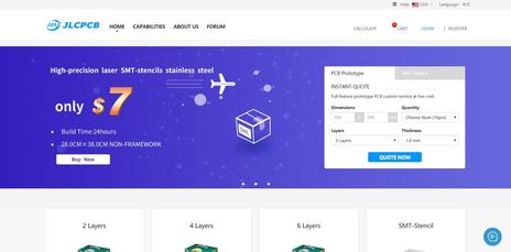
After searching for many PCB (Printed Circuit Board) fabrication services and companies with reasonable pricing and offers, I came across JLCPCB, a professional PCB fabrication service with lots of selections to choose from. I first found this company from multiple sources, which includes advertisements, videos, blogs and other articles. It was known to be very inexpensive and affordable for any maker to order a custom PCB. Upon visiting JLCPCB’s website, I was immediately immersed into all of their awesome services and attractive prices. Even navigating through their website was fairly easy for someone who isn’t skillful in the PCB field, and a price could be quoted without the need to register or log in to an account.
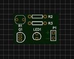
To start of with the process of printing a PCB, I first designed my project’s schematics and my custom PCB using a cloud-based software called EasyEDA. The project I wanted to transform from a breadboard to a PCB was a simple night light, utilizing an LDR (Light Dependant Resistor) and a LED (Light Emitting Diode) as well as other assisting components. I chose a fairly easy project to start with, as I now know that I can even transform a major project to a PCB effortlessly. Once I am done creating the schematics for this project, I customise my PCB and generate a gerber file. In EasyEDA, I can view what my PCB will you look like immediately after creating the PCB. A very positive aspect of EasyEDA is that I can be redirected to JLCPCB’s site without any hesitation as it is one of EasyEDA’s menu selection features.
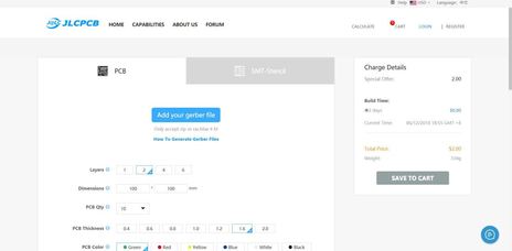
Once I am in JLCPCB’s website, it gets really easy from there. I create my own account, with the option of using my email, and I can upload the gerber file as generated from EasyEDA on this page. I click the “Add your gerber file” button on that page, select my file and click the blue button located there. The .zip and .rar file formats are only accepted, with a maximum size of 4M, so you can upload much larger PCBs to print. From there, the website gives you functions to customize your PCB specifications like the: amount of layers, dimensions of the PCB, quantity, PCB thickness, PCB colour, finishes, etc. There is even an option to add an additional laser stancil to go with your custom PCB and remarks if you need anything extra. My favourite part of the JLCPCB site is that, when you upload your gerber file, you can get to see a sneak preview of its physical appearance with the settings you have set. The price is also shown on the right of that page and you can see the prices altered if you made changes to the PCB settings. You can press the “Save to Cart” button after you are satisfied with what your PCB’s specifications are and proceed to the final checkout page. These factors of JLCPCB makes my life really easy as I don’t need to navigate around its website when everything I need, is all shown on one page. Next, the shipping and payment processes will take place.
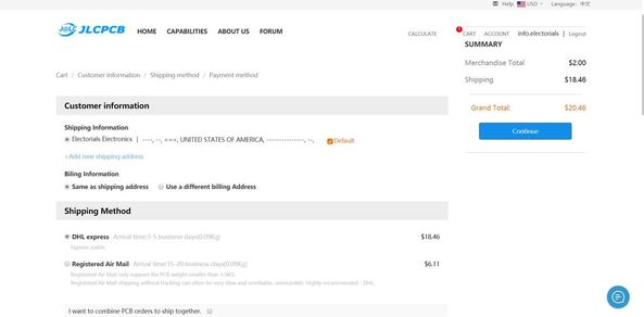
After the selection and customisation of your PCB as said in my last article, the next step for this simple PCB design process is the payment, and shipping. The payment process is simple to make with two different methods: ‘review before payment’ and ‘direct payment’. The first method, ‘review before payment’, is where you can pay for the PCB after its design file is generated, then reviewed. It can only take 10 minutes on working days (Monday - Friday 9am - 6pm GMT+8), but, the production of the PCB will only take place once the payment is received by JLCPCB. On the other hand, you can pay before the PCB design file will be reviewed to ensure the high efficiency of your PCB production. However, if your file can’t be approved using this method, you will have a refund of what you paid for. This payment method is recommend to makers who want their product to be fast and convenient for them. Now, moving on to the shipping, there are also two shipping methods available. JLCPCB provides an express shipping with DHL Express or, regular mail by Registered Air Mail. Of course, DHL Express will cost you a bit extra to pay for as their shipping time can take 3 -5 days only, where the Registered Air Mail is cheaper, but will take 15 - 20 days. I would highly recommend DHL Express for makers with urgent orders or requests, and Registered Air Mail for orders which allows some time to be delivered. But, you can choose your preferable shipping method based on what you feel is best. On that same website page, you can set your shipping and billing address as well. With those final specifications set, the final price will be set and you can pay in the next few pages without any hesitation by using PayPal or a bank transfer with MasterCard or VISA. JLCPCB’s easy website design ensures that there will be no confusion when ordering your PCB and you can follow the steps, which is clearly shown, to complete this full process by yourself.
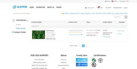
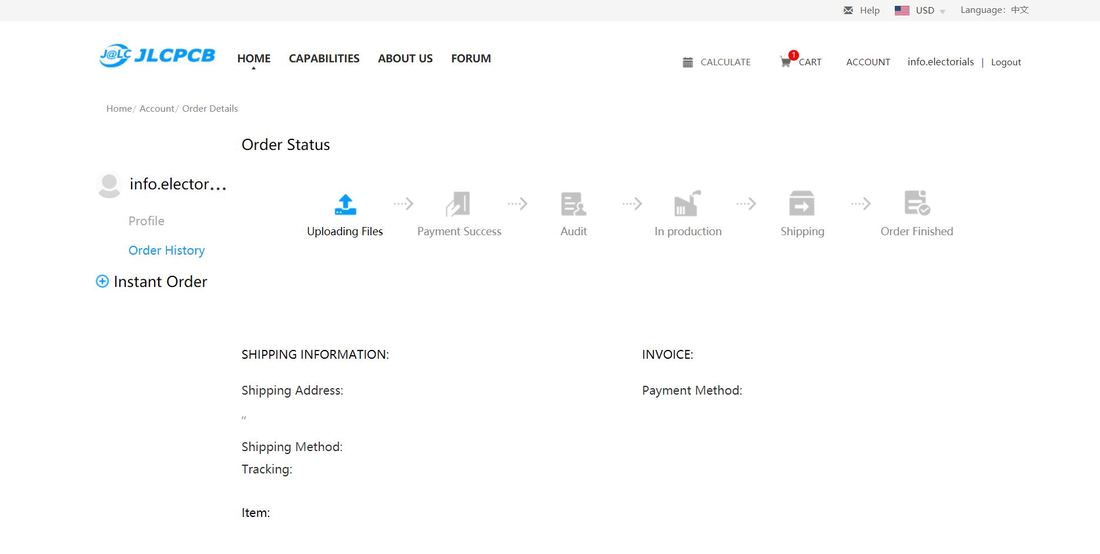
From the final click of the checkout button, you can immediately see a tracking page of your order, step-by-step, by clicking on “Account” on the top right corner of JLCPCB’s website. On that page, you can find your current, processing orders, or your order history with all of your past orders. By clicking on any order, you can find a variety of details, such as the payment invoice, the shipping tracking information, the time of when the PCB was being produced, and much more. This is a nice characteristic of ordering your PCB from JLCPCB, as you can be assured that every step of the production process goes smoothly and that you can inquire if there is a series of unexpected events occuring, like a manufacturing fault from the start, or a delivery issue when shipping.
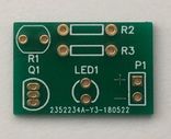
Now, let’s get through to the actual custom PCBs I have ordered from JLCPCB. It came in around 3 days with DHL Express and the packaging was decent, with the PCBs packed in a plastic bag, undamaged. Upon close observations, I noticed that these boards were excellently made and it was polished very well. The coating looked amazing and, overall, its aesthetics were attractive to anyone. I think that the white text in the PCB design really stood out from the PCB itself, and it can be seen clearly to anybody soldering. In regards to the texture, the board was pretty smooth to the touch and didn’t have any rough edges or surfaces at all. These impressive factors also applied to the 9 other PCBs I have ordered which are exactly identical to each other. You could see one of my ordered PCBs in the image below upon arrival and out of its package bag. In my next article, you can see the PCBs soldered up and a comprehensive review of what I think about the PCBs. You can be directed to my next article by clicking here.
