An astable multivibrator circuit is one of the most basic, simple electronic circuits to work with as it requires a few components, the circuit is easy to understand and creating the circuit on a breadboard or on a PCB (Printed Circuit Board) is effortless. It is a type of relaxation oscillator which is essentially a relative to the monostable or bistable multivibrator, but this circuit does not require any type of external trigger pulse for it to function properly. In terms of this circuit visually, the output represents a common LED (Light Emitting Diode) flasher/oscillator circuit with two LEDs blinking alternately. When one LED blinks, the other doesn't blink and vice versa. Let's quickly take a look at the schematics of this simple circuit. I have done a quick sketch of its schematics in EasyEDA:
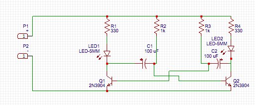
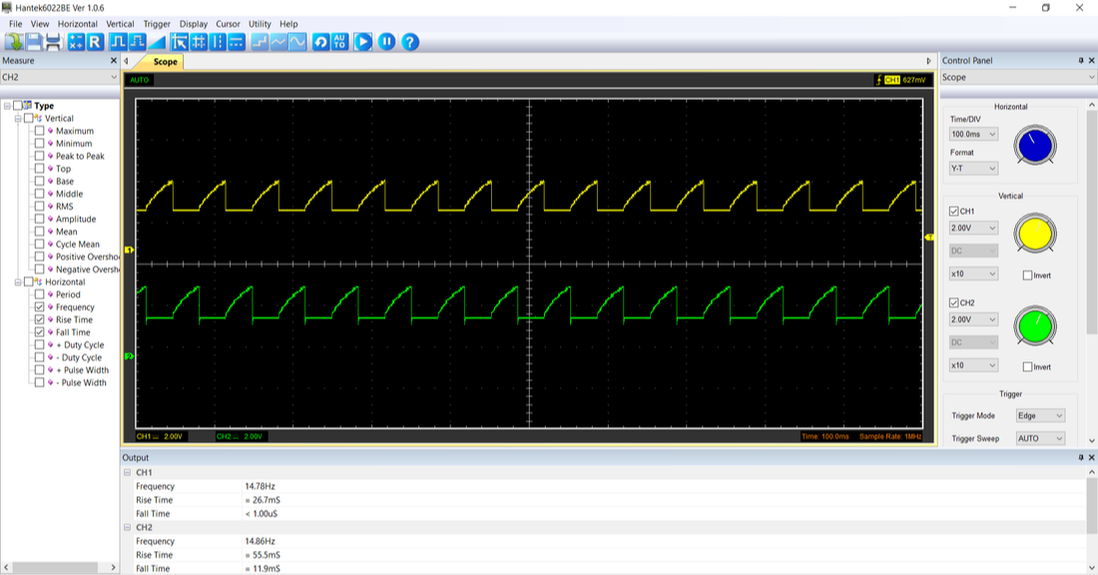
As you can see in the above image, this circuit comprises of two LEDs, two capacitors, two resistors for the LEDs, two resistors for the charging of the capacitor and a DC +9 volt power supply. This circuit actually produces a continuous square wave output, where the frequency is mainly determined by the capacitance of the delay capacitor in the circuit and the resistance of R2 and R3, which are responsible for charging the capacitor. This specific charging/discharging circuit is known as an RC circuit. However, they must be of the same value to make this circuit work with the LED blinking in equal phases. Plus, with this square wave output, you could use it to run circuits, feed it to a speaker to make sounds or for simply strobing it. At first glance, you can clearly see that the transistors are cross-coupled in a certain way, where their gates are connected to the negative leg of a capacitor on the opposite side. This is the main cause to why the LED can switch back and forth repeatedly in two states, a high state and a low state. Both transistors are biased for linear operation and are used as Common Emitter Amplifiers with a full positive feedback, and when one is on, the other is off. This picture below shows the frequency of the two LEDs blinking:
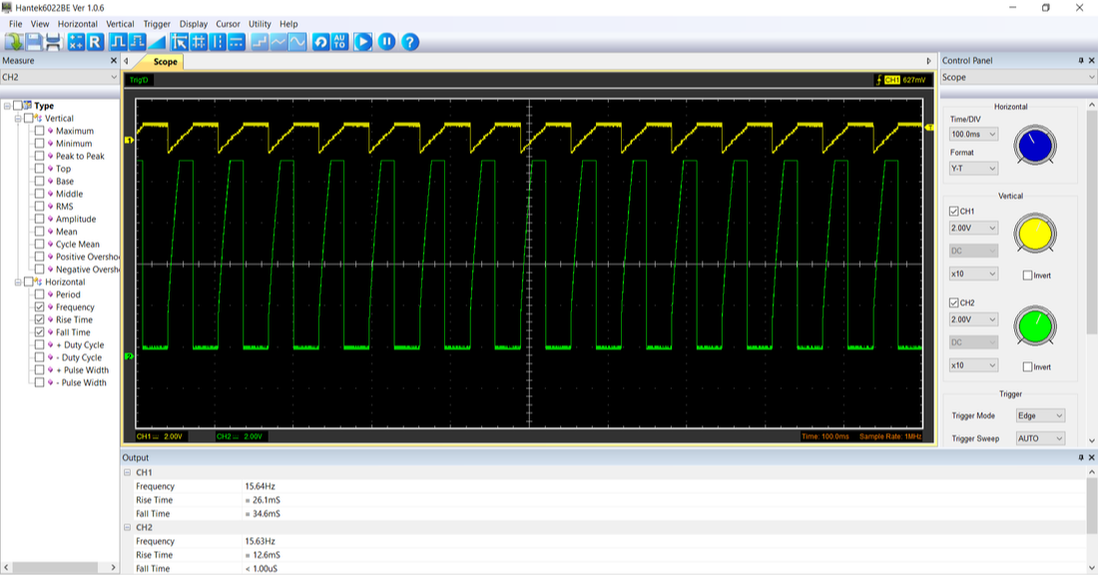
When Q1 is turned on, its collector will be at zero volts, as well as C1, because Q2 is turned off with its collector at the supply voltage and its base also at zero volts (same as Q1) due to C1 not being charged. Then, as C1 begins to charge via R2 to a potential of about +0.6 volts, Q2 will be conducting heavily due to its connection to C1. As the current to the collector of Q2 begins to increase, this causes a voltage drop across R4 to make the collector voltage of Q2 fall as well, causing C2 to fall additionally. Since our input power supply is +9 volts and transistor Q1's base is conducting, the base voltage would be around +0.6 volts, so when Q2 conducts, Q1's base falls to around -8.4 volts as it is the amplification voltage (+0.6 volts) minus the supply voltage (+9 volts). When this happens, it turns off Q1 to cause a rise in its collector voltage. This then makes Q2 turn on as Q1 turns off, causing alternate states at both outputs. For the next sequence after, C2 will now be charged once the base voltage of Q1 reaches +0.6 volts. This whole process causes the collector and base waveforms as seen by the images down below:
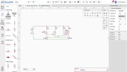
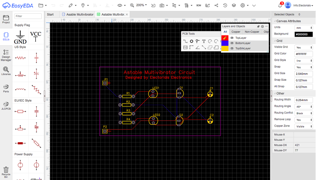
You can also further extend this circuit from just looking at some schematics and a circuit diagram to professionally manufacturing a PCB with FSPCB. Since I had an idea of the schematics in mind, I decided to start by placing the schematics onto EasyEDA by tracing them out normally. Any other PCB design software, such as Eagle, can be used. Then, I used an automatic function to fabricate the schematic design onto a PCB, all in the EasyEDA software. From here, I easily sorted the components out on the PCB and placed them in positions which I think are practical and suitable. After that, I routed the tracks of every component using the auto-routing feature, which is another feature of EasyEDA.
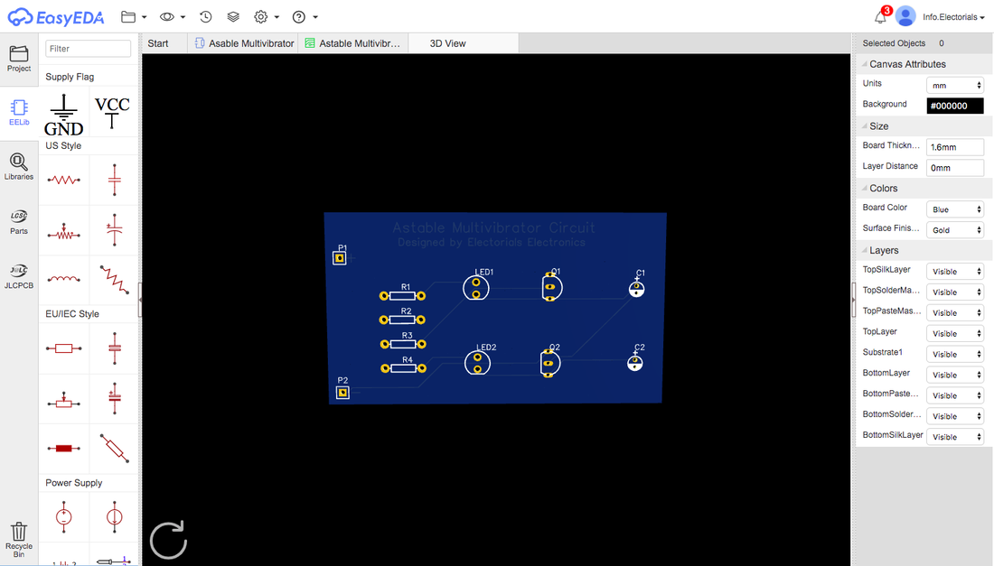
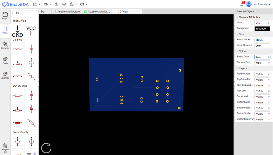
For the power input, I placed some empty pads, mounted onto the PCB, so I can insert the input wires of a +9 volt battery pack, or jumper wires directly from a +9 volt power supply. It is also helpful to place positive (+) and negative (-) markings next to their respective hole so that you won't mess up the polarity of power when applying a voltage to this circuit and during soldering. In the image of my designed PCB above, some of the tracks were placed at the back of the PCB, due to track crossings and this just makes it a neater, cleaner design overall. I have also specifically tried to make all the components symmetrical to each other so that there will be no confusion upon knowing how the components are all connected to each other. The set of resistors is also lined up symmetrically vertically so that I can identify which PCB goes to which component without any hesitation. Other than those specific aspects, this is really a basic PCB to follow where you can put your own placement of components anywhere, as long as the routing is set properly. Once I have designed my PCB and finalised it, EasyEDA has a built-in PCB 3D viewer function to demonstrate what your PCB is like after the design process is over. You can also change the features of the 3D viewer for you to visualize what your PCB looks like with a red, green, or blue solder mask colour. This applies to the silkscreen colour, for example, as you can change between gold and silver. There are also other interesting features of a PCB.
After that, I can just download my Gerber file directly from my PCB design software and upload it to the website of my chosen PCB fabrication company. Typically, after uploading your Gerber file, there are several customisation options for your PCB, such as options for PCB colour, surface finish, copper weight, gold fingers etc. This is where you can customize your PCB to your own liking by altering the track materials used, no. of boards, and surface finish in addition to the PCB colour (silkscreen).
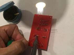
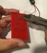
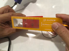
Once my PCBs arrived, I went straight to the soldering of the boards since I had the necessary components on hand already, the pictures below are what my soldering looks like. I have to say though, the component holes were ideal for solder as it just flowed well once the heat was applied to the pad. This led to all of the components being held down well and firmly in place. Anyways, the pictures of the soldering and clipping of component legs being done are shown below. I additionally used a magnifying ruler to examine the solder joints to ensure that everything was soldered on well and the legs are clipped off with perfection. It is important to look over all the solder joints you have made after soldering to see if any solder bridges have been made, which may damage components or destroy the circuitry completely.
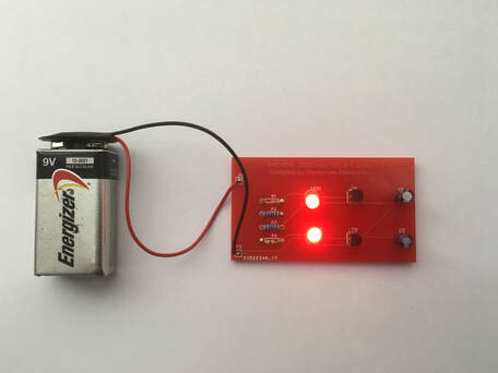
Finally, this is my finished PCB, all completely soldered up, cleaned and working as expected. The picture below shows the two LEDs blinking together, even though it is blinking alternately, as the camera cannot pick up the fast frequency which the two LEDs are running under. But, you can go ahead and switch the resistors and capacitors around to different values as part of the RC circuit as you will then see differences in frequency.

